Custom LD & TEC Drivers
The preferred solution to drive the laser in the Performance Edition is to use the custom LD & TEC Drivers circuit. The complete CAD and Bill of Materials to reproduce the circuit can be downloaded here:
Download the files here: LD & TEC Drivers (rev2).
The circuit is built around the “old-school” through-holes technology and requires no specific skills or tools apart from a temperature-controlled soldering gun. If you don’t own one, I recommend the Weller PU 81 which I use for all my circuits. An oscilloscope is also recommended but not mandatory. The circuit can be reproduced under 500€ ex-VAT but requires some extra tooling such as Thorlabs MTD evaluation board.
When you order the PCB, I recommend a 1.5 mm board thickness and a minimum width of 35 µm copper thickness. Selective gold plating can also make your life easier and I systematically add it to my orders. Be aware though that gold will dissolve in the solder and make it more fragile in the long term. Also, gold plated PCBs do not desolder pretty well.
The final assembled circuit is shown below. I will guide you step by step to make it.
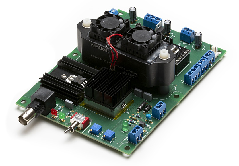
The Bill Of Materials will tell you what to solder where. Respect carefully the number and orientation of the components.
Start by soldering the resistors. Bend the legs at 90° before putting them in the PCB. Solder the legs vertically, not with an angle. Resistors do not have a specific orientation but you want to make sure that they stand flat on the PCB for a nicer look. Cut the legs of the resistors once they are soldered (one resistor at a time) paying attention to flying wires. I recommend holding the upper side of the legs as you cut them.
Then solder the ICs ILD1, CB4082 and TL084. Be aware that ICs are delicate circuits that can be sensitive to ESD so you must wear ESD protection devices at all times when handling them. Also, ICs have an orientation, so you need to check the small “U”-shaped groove mark on top of them and align the marking with the one drawn on the PCB. Note that you may need to bend slightly the legs to be able to insert them into the PCB. Use a clean block of metal to bend them at once using finger pressure.
You can now solder the diodes except the LEDs. Diodes are also sensitive to ESD and also have an orientation to respect. Align the “|” mark of the diodes with the PCB.
Solder the 1 µF and 22 µF capacitors. They don’t have a specific orientation. Then solder the trimmers RV1 and RV2. Continue by soldering all the 100 nF capacitors, the toggle switch, and the header blocks. The idea is to progress by height so that all elements are in good contact with the PCB board and you don’t have one hanging above the tracks.
You can also solder the LEDs, the BC557 transistor, and the 7808 regulator. Take care that all these elements have an orientation and that the BC557 and 7808 are sensitives to ESD. The (+) side of the LEDs correspond to their longest leg.
You may then finish by soldering the 100 µF capacitors, the BNC connector, and attach the spacer/raiser blocks. The 100 µF capacitors have an orientation so you should align the (+) side correctly. Usually, capacitors shows the (-) side on their housing as a band with “- – -” written on them.
The negative regulator 7908 requires a bit more work as shown in the picture:
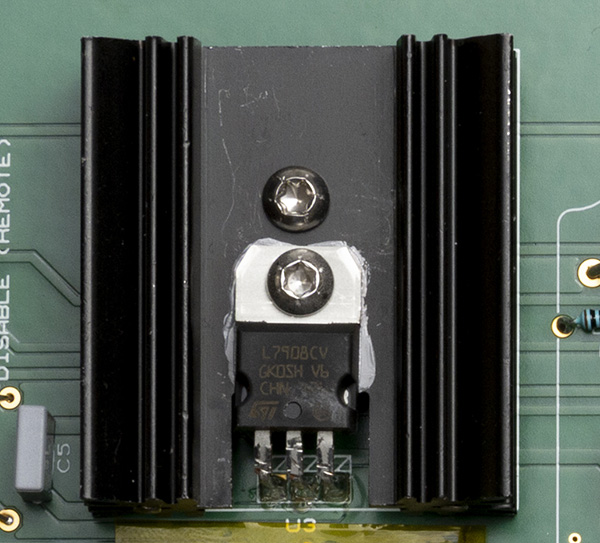
The regulator needs to be attached to a heatsink with one gentle drop of thermal paste correctly squeezed between the two. The thermal paste should make a thin but uniform layer between the two surfaces in contact. Do NOT put excessive paste as it will hinder the performance of the heat transfer. Secure the regulator to the heatsink using a DIN912 M3×4 plastic screw (the screw in the picture is a bit different because I did not have plastic screws at the time of assembly). Secure the heatsink using a DIN912 M3×12 plastic screw with a plastic washer and solder the legs as shown in the picture. Take care that lead do not short-circuit.
The MOSFET transistor Q1 requires a bit more work as well. You will have to machine (or order) the custom block #2020-20/1 out of aluminum (STEP files and drawings given with the circuit download files). The “APF30-30-13CB” heatsink is placed on top of the block and secured using epoxy glue (I used Scotchweld 2216 but you can use a different one). Thermal contact between the two surfaces is made using thermal paste. Again, the paste should be squeezed to a uniform thin film between the two surfaces.
When assembling the heatsink to the aluminum block, pay attention to the orientation. You should put the heatsink to the opposite side of the small threaded hole at the base of the block.
The MOSFET is put in contact with the block using some gentle thermal paste one more time. It is held in place using a M3×5 DIN913 set screw. Do not force on the set screw. Also, MOSFET are ESD-sensitive devices so you should wear ESD protection at all times during this process.
Attach the block to the PCB using a DIN912 M4×8 plastic screw and bend the legs using a pair of pliers as shown in the picture here below:
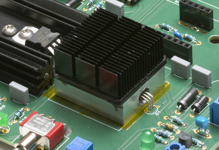
Note that I also added some Kapton tape below the aluminum block. This is mandatory to protect shorting the vias on the PCB.
Your circuit is now ready to be tested!
Connect your power supply to the header block respecting the GND for the 5V and +/-12V parts as they are isolated in the power supply module. Turn the power supply on. Turn it off immediately if you notice anything odd (e.g. noise, burnt smell etc.).
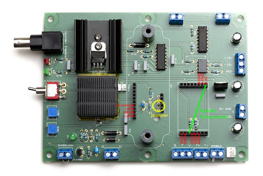
Using a quality voltmeter or oscilloscope, check all the voltage pins as shown in the figure here-below:
Connect your voltmeter GND probe to the power supply GND and test each lead for the correct voltage. Remember that the 5V and 12V grounds are isolated so you need to use the 12V ground to test the left-hand-side part of the circuit and the 5V to test the right-hand-side part of the circuit.
You can now adjust the default current settings on the board. Connect your voltmeter to the GND and Vcontrol pins. Flip the toggle switch to the first position and slowly turn the first trimmer until the voltage reads 660 mV. This will set the current to 330 mA which should be a safe value to use with a DJ532-40 laser diode. Toggle the switch to the second position and adjust the trimmer to read 350 mV. This should adjust the current to 175 mA. During operations, I use the second current setting for alignment purposes and tune the trimmer down until the laser is comfortable for the eyes (<1 mW).
Before testing the LD3000R, first solder a jumper wire as indicated in yellow in the previous image. This is required by the LD3000R for external current operation.
Warning: the LD3000R can be destroyed by connecting it to an improperly-set jumper wire (or no jumper wire in place) so double-check this!
With the power supply off, put the LD3000R in place and secure it using M4×20 DIN912 plastic screws sand #8 washers. Connect three 1N4001 diodes attached in series between the A and K connectors respecting the polarity (“|” marks oriented to the K side). Pay attention that all these elements (including the LD3000R) are ESD sensitive.
Add a jumper wire to the interlock and connect the key switch to the enable header blocks. Add a jumper wire to bypass the MTD415TE as shown in green in the previous picture.
Connect your voltmeter or oscilloscope to the A/K header block and power on the power supply. You should see the voltage go from ~0V to ~2V as you switch on and off the key switch. Repeat the experiment with the two positions of the current selector switch.
If all the tests went fine, you can now connect the MTD415TE paying attention to its orientation as shown in the picture here below. Take care that the IC is sensitive to ESD.
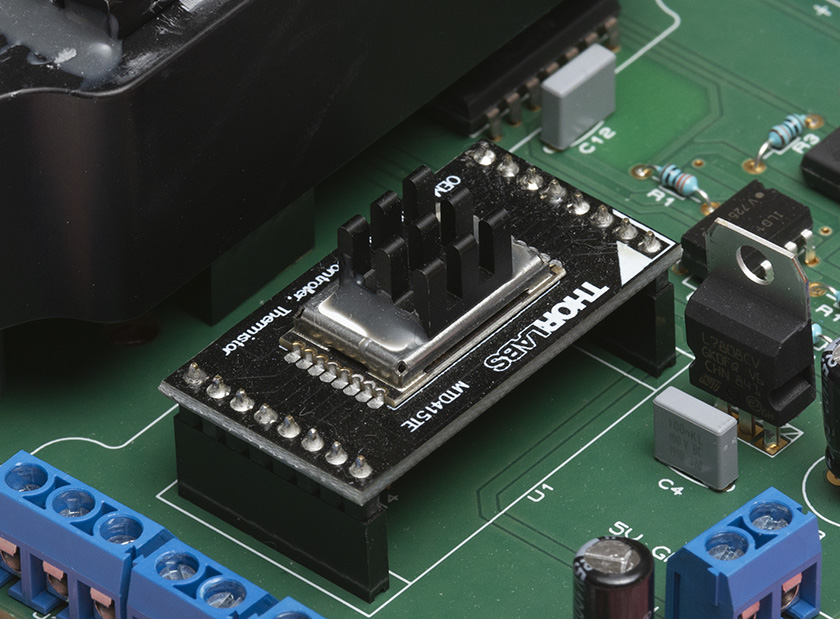
You will notice that I fixed a small additional heatsink to the MTD415TE to be safe. Once again, use a thin layer of thermal paste and secure it using epoxy glue.
Similarly, I attached some active cooling to the LD3000R. Tests have shown that this might not be necessary at 400 mA but you can implement it as well if you feel more confident with it.
Also, do not forget to attach a “FEX40-40-21/T710/M2” active cooling heatsink system to your LDM21 block and connect this to the IC circuit with the correct polarity. This cooling is not optional as it is required to avoid overloading the TEC element when operating the laser for more than 10 minutes.
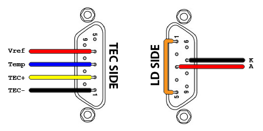
Before you can test your laser, you will have to wire it to the LDM21 using SUB-D9 connectors. I recommend using 18AWG cables for all power lines and a twisted/shielded pair to connect the temperature sensing part. The circuit has a “shield” connection port to connect the bread of the shield. The cable shield must be connected on one side only (circuit-side).
Cable the connectors as follow (image as seen from the rear side of the LDM21 block):
Before connecting the MTD415TE to the circuit board you will have to configure it. This can be done using Thorlabs MTDEVAL evaluation board and a Windows computer. The laser can remain unplugged during the configuration of the board.
Connect all the wires and the USB cable to the evaluation board before powering it on. Note that for some reason the TEC+ and TEC- ports have to be inverted.
Install Thorlabs evaluation software and start the application. Connect to the evaluation board and copy the following settings:
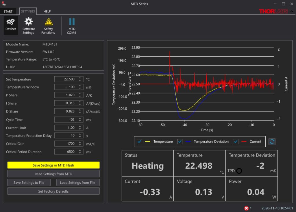
The temperature should stabilize to the set point without oscillation, as shown in the picture. Note that I recommend increasing the Temperature Window to 250 mK (image shows 100 mK). You may also fine tune your PID settings using the procedure described in Thorlabs datasheet but the values given here should already be a good approximation for your setup.
Save the settings in the MTD flash and unplug/poweroff the evaluation board.
You should now be able to test your laser.
Make sure the key switch is in the “OFF” position and power on the circuit. Wait 1 minute for the TEC to settle to its set point. Check that the toggle switch is on the 330 mA setting and turn the key switch on. The laser should start in about 2 seconds. Switch the key off and check that the laser stops instantaneously. Toggle the switch to the second position and perform the same test. Eventually adapt the trimmer set point gently if the laser is too dim (or not visible) or too bright. Do not turn more than 1 turn as you may overdrive the laser. Turn the key switch off and unplug the power supply.
Warning: To protect your laser, always make sure that the key switch is set to the “OFF” position as you power on and off the circuit.
Note concerning the Remote Disable port:
The circuit implements an isolated remote disable BNC port. The laser can be turned off by sending a +5V signal to the port (polarity: inside pin is (+)). No protections are included so check that your signal is +5V +/-10%.
The laser will be off if at least one of the following conditions are met:
- A +5V is present on the Remote Disable Port
- The key switch is set to “OFF”
- The interlock switch is open
- The LDM21 temperature is outside the temperature range